MIT_8086
8086 microprocessor
Intel 8086
- Intel 8086 microprocessor is the enhanced version of Intel 8085 microprocessor. It was designed by Intel in 1976.
- The 8086 microprocessor is a16-bit, N-channel, HMOS microprocessor. Where the HMOS is used for "High-speed Metal Oxide Semiconductor".
- Intel 8086 is built on a single semiconductor chip and packaged in a 40-pin IC package. The type of package is DIP (Dual Inline Package).
- Intel 8086 uses 20 address lines and 16 data- lines. It can directly address up to 220 = 1 Mbyte of memory.
- It consists of a powerful instruction set, which provides operation like division and multiplication very quickly.
- 8086 is designed to operate in two modes, i.e., Minimum and Maximum mode.
Difference between 8085 and 8086 Microprocessor
| 8085 Microprocessor | 8086 Microprocessor |
|---|---|
| It is an 8-bit microprocessor. | It is a 16-bit microprocessor. |
| It has a 16-bit address line. | It has a 20-bit address line. |
| It has a 8-bit data bus. | It has a 16-bit data bus. |
| The memory capacity is 64 KB. | The memory capacity is 1 MB. |
| The Clock speed of this microprocessor is 3 MHz. | The Clock speed of this microprocessor varies between 5, 8 and 10 MHz for different versions. |
| It has five flags. | It has nine flags. |
| 8085 microprocessor does not support memory segmentation. | 8086 microprocessor supports memory segmentation. |
| It does not support pipelining. | It supports pipelining. |
| It is accumulator based processor. | It is general purpose register based processor. |
| It has no minimum or maximum mode. | It has minimum and maximum modes. |
| In 8085, only one processor is used. | In 8086, more than one processor is used. An additional external processor can also be employed. |
| It contains less number of transistors compare to 8086 microprocessor. It contains about 6500 transistor. | It contains more number of transistors compare to 8085 microprocessor. It contains about 29000 in size. |
| The cost of 8085 is low. | The cost of 8086 is high. |
8086 pins configuration
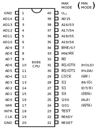
The description of the pins of 8086 is as follows:
AD0-AD15 (Address Data Bus): Bidirectional address/data lines. These are low order address bus. They are multiplexed with data.
When these lines are used to transmit memory address, the symbol A is used instead of AD, for example, A0- A15.
A16 - A19 (Output): High order address lines. These are multiplexed with status signals.
A16/S3, A17/S4: A16 and A17 are multiplexed with segment identifier signals S3 and S4.
A18/S5: A18 is multiplexed with interrupt status S5.
A19/S6: A19 is multiplexed with status signal S6.
BHE/S7 (Output): Bus High Enable/Status. During T1, it is low. It enables the data onto the most significant half of data bus, D8-D15. 8-bit device connected to upper half of the data bus use BHE signal. It is multiplexed with status signal S7. S7 signal is available during T3 and T4.
RD (Read): For read operation. It is an output signal. It is active when LOW.
Ready (Input): The addressed memory or I/O sends acknowledgment through this pin. When HIGH, it denotes that the peripheral is ready to transfer data.
RESET (Input): System reset. The signal is active HIGH.
CLK (input): Clock 5, 8 or 10 MHz.
INTR: Interrupt Request.
NMI (Input): Non-maskable interrupt request.
TEST (Input): Wait for test control. When LOW the microprocessor continues execution otherwise waits.
VCC: Power supply +5V dc.
GND: Ground.
Operating Modes of 8086
There are two operating modes of operation for Intel 8086, namely the minimum mode and the maximum mode.
When only one 8086 CPU is to be used in a microprocessor system, the 8086 is used in the Minimum mode of operation.
In a multiprocessor system 8086 operates in the Maximum mode.
Pin Description for Minimum Mode
In this minimum mode of operation, the pin MN/MX is connected to 5V D.C. supply i.e. MN/MX = VCC.
The description about the pins from 24 to 31 for the minimum mode is as follows:
INTA (Output): Pin number 24 interrupts acknowledgement. On receiving interrupt signal, the processor issues an interrupt acknowledgment signal. It is active LOW.
ALE (Output): Pin no. 25. Address latch enable. It goes HIGH during T1. The microprocessor 8086 sends this signal to latch the address into the Intel 8282/8283 latch.
DEN (Output): Pin no. 26. Data Enable. When Intel 8287/8286 octal bus transceiver is used this signal. It is active LOW.
DT/R (output): Pin No. 27 data Transmit/Receives. When Intel 8287/8286 octal bus transceiver is used this signal controls the direction of data flow through the transceiver. When it is HIGH, data is sent out. When it is LOW, data is received.
M/IO (Output): Pin no. 28, Memory or I/O access. When this signal is HIGH, the CPU wants to access memory. When this signal is LOW, the CPU wants to access I/O device.
WR (Output): Pin no. 29, Write. When this signal is LOW, the CPU performs memory or I/O write operation.
HLDA (Output): Pin no. 30, Hold Acknowledgment. It is sent by the processor when it receives HOLD signal. It is active HIGH signal. When HOLD is removed HLDA goes LOW.
HOLD (Input): Pin no. 31, Hold. When another device in microcomputer system wants to use the address and data bus, it sends HOLD request to CPU through this pin. It is an active HIGH signal.
Pin Description for Maximum Mode
In the maximum mode of operation, the pin MN/¯MX is made LOW. It is grounded. The description about the pins from 24 to 31 is as follows:
QS1, QS0 (Output): Pin numbers 24, 25, Instruction Queue Status. Logics are given below:
| QS1 | QS0 | Operation |
|---|---|---|
| 0 | 0 | No operation |
| 0 | 1 | 1st byte of opcode from queue. |
| 1 | 0 | Empty the queue |
| 1 | 1 | Subsequent byte from queue |
S0, S1, S2 (Output): Pin numbers 26, 27, 28 Status Signals. These signals are connected to the bus controller of Intel 8288. This bus controller generates memory and I/O access control signals. Logics for status signal are given below:
| S2 | S1 | S0 | Operation |
|---|---|---|---|
| 0 | 0 | 0 | Interrupt acknowledgement |
| 0 | 0 | 1 | Read data from I/O port |
| 0 | 1 | 0 | Write data from I/O port |
| 0 | 1 | 1 | Halt |
| 1 | 0 | 0 | Opcode fetch |
| 1 | 0 | 1 | Memory read |
| 1 | 1 | 0 | Memory write |
| 1 | 1 | 1 | Passive state |
LOCK (Output): Pin no. 29. It is an active LOW signal. When this signal is LOW, all interrupts are masked and no HOLD request is granted. In a multiprocessor system all other processors are informed through this signal that they should not ask the CPU for relinquishing the bus control.
RG/GT1, RQ/GT0 (Bidirectional): Pin numbers 30, 31, Local Bus Priority Control. Other processors ask the CPU by these lines to release the local bus.
In the maximum mode of operation signals WR, ALE, DEN, DT/R etc. are not available directly from the processor. These signals are available from the controller 8288.
Functional units of 8086
8086 contains two independent functional units: a Bus Interface Unit (BIU) and an Execution Unit (EU).
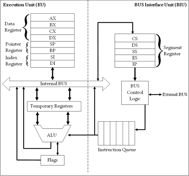
Fig: Block Diagram of Intel 8086 Microprocessor (8086 Architecture)
Bus Interface Unit (BIU)
The segment registers, instruction pointer and 6-byte instruction queue are associated with the bus interface unit (BIU).
The BIU:
- Handles transfer of data and addresses,
- Fetches instruction codes, stores fetched instruction codes in first-in-first-out register set called a queue,
- Reads data from memory and I/O devices,
- Writes data to memory and I/O devices,
- It relocates addresses of operands since it gets un-relocated operand addresses from EU. The EU tells the BIU from where to fetch instructions or where to read data.
It has the following functional parts:
- Instruction Queue: When EU executes instructions, the BIU gets 6-bytes of the next instruction and stores them in the instruction queue and this process is known as instruction pre fetch. This process increases the speed of the processor.
- Segment Registers: A segment register contains the addresses of instructions and data in memory which are used by the processor to access memory locations. It points to the starting address of a memory segment currently being used.
There are 4 segment registers in 8086 as given below:- Code Segment Register (CS): Code segment of the memory holds instruction codes of a program.
- Data Segment Register (DS): The data, variables and constants given in the program are held in the data segment of the memory.
- Stack Segment Register (SS): Stack segment holds addresses and data of subroutines. It also holds the contents of registers and memory locations given in PUSH instruction.
- Extra Segment Register (ES): Extra segment holds the destination addresses of some data of certain string instructions.
- Instruction Pointer (IP): The instruction pointer in the 8086 microprocessor acts as a program counter. It indicates to the address of the next instruction to be executed.
Execution Unit (EU)
- The EU receives opcode of an instruction from the queue, decodes it and then executes it. While Execution, unit decodes or executes an instruction, then the BIU fetches instruction codes from the memory and stores them in the queue.
- The BIU and EU operate in parallel independently. This makes processing faster.
- General purpose registers, stack pointer, base pointer and index registers, ALU, flag registers (FLAGS), instruction decoder and timing and control unit constitute execution unit (EU). Let's discuss them:
- General Purpose Registers: There are four 16-bit general purpose registers: AX (Accumulator Register), BX (Base Register), CX (Counter) and DX. Each of these 16-bit registers are further subdivided into 8-bit registers as shown below:
| 16-bit registers | 8-bit high-order registers | 8-bit low-order registers |
|---|---|---|
| AX | AH | AL |
| BX | BH | BL |
| CX | CH | CL |
| DX | DH | DL |
- Index Register: The following four registers are in the group of pointer and index registers:
- Stack Pointer (SP)
- Base Pointer (BP)
- Source Index (SI)
- Destination Index (DI)
- ALU: It handles all arithmetic and logical operations. Such as addition, subtraction, multiplication, division, AND, OR, NOT operations.
- Flag Register: It is a 16?bit register which exactly behaves like a flip-flop, means it changes states according to the result stored in the accumulator. It has 9 flags and they are divided into 2 groups i.e. conditional and control flags.
- Conditional Flags: This flag represents the result of the last arithmetic or logical instruction executed. Conditional flags are:
- Carry Flag
- Auxiliary Flag
- Parity Flag
- Zero Flag
- Sign Flag
- Overflow Flag
- Control Flags: It controls the operations of the execution unit. Control flags are:
- Trap Flag
- Interrupt Flag
- Direction Flag
- Conditional Flags: This flag represents the result of the last arithmetic or logical instruction executed. Conditional flags are:
Interrupts
Interrupt is a process of creating a temporary halt during program execution and allows peripheral devices to access the microprocessor.
Microprocessor responds to these interrupts with an interrupt service routine (ISR), which is a short program or subroutine to instruct the microprocessor on how to handle the interrupt.
There are different types of interrupt in 8086:
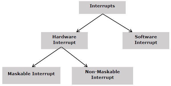
Hardware Interrupts
Hardware interrupts are that type of interrupt which are caused by any peripheral device by sending a signal through a specified pin to the microprocessor.
The Intel 8086 has two hardware interrupt pins:
- NMI (Non-Maskbale Interrupt)
- INTR (Interrupt Request) Maskable Interrupt.
NMI: NMI is a single Non-Maskable Interrupt having higher priority than the maskable interrupt.
- It cannot be disabled (masked) by user using software.
- It is used by the processor to handle emergency conditions.
For example: It can be used to save program and data in case of power failure. An external electronic circuitry is used to detect power failure, and to send an interrupt signal to 8086 through NMI line.
INTR: The INTR is a maskable interrupt. It can be enabled/disabled using interrupt flag (IF). After receiving INTR from external device, the 8086 acknowledges through INTA signal.
It executes two consecutive interrupt acknowledge bus cycles.
Software Interrupt
A microprocessor can also be interrupted by internal abnormal conditions such as overflow; division by zero; etc. A programmer can also interrupt microprocessor by inserting INT instruction at the desired point in the program while debugging a program. Such an interrupt is called a software interrupt.
The interrupt caused by an internal abnormal conditions also came under the heading of software interrupt.
Example of software interrupts are:
- TYPE 0 (division by zero)
- TYPE 1 (single step execution for debugging a program)
- TYPE 2 represents NMI (power failure condition)
- TYPE 3 (break point interrupt)
- TYPE 4 (overflow interrupt)
Interrupt pointer table for 8086
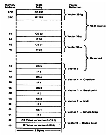
Fig: Interrupt pointer table for 8086
The 8086 can handle up to 256, hardware and software interrupts.
1KB memory acts as a table to contain interrupt vectors (or interrupt pointers), and it is called interrupt vector table or interrupt pointer table. The 256 interrupt pointers have been numbered from 0 to 255 (FF hex). The number assigned to an interrupt pointer is known as type of that interrupt. For example, Type 0, Type 1, Type 2,...........Type 255 interrupt.
Addressing modes of 8086
The way for which an operand is specified for an instruction in the accumulator, in a general purpose register or in memory location, is called addressing mode.
The 8086 microprocessors have 8 addressing modes. Two addressing modes have been provided for instructions which operate on register or immediate data.
These two addressing modes are:
Register Addressing: In register addressing, the operand is placed in one of the 16-bit or 8-bit general purpose registers.
Example
- MOV AX, CX
- ADD AL, BL
- ADD CX, DX
Immediate Addressing: In immediate addressing, the operand is specified in the instruction itself.
Example
- MOV AL, 35H
- MOV BX, 0301H
- MOV [0401], 3598H
- ADD AX, 4836H
The remaining 6 addressing modes specify the location of an operand which is placed in a memory.
These 6 addressing modes are:
Direct Addressing: In direct addressing mode, the operand?s offset is given in the instruction as an 8-bit or 16-bit displacement element.
Example
- ADD AL, [0301]
The instruction adds the content of the offset address 0301 to AL. the operand is placed at the given offset (0301) within the data segment DS.
Register Indirect Addressing: The operand's offset is placed in any one of the registers BX, BP, SI or DI as specified in the instruction.
Example
- MOV AX, [BX]
It moves the contents of memory locations addressed by the register BX to the register AX.
Based Addressing: The operand's offset is the sum of an 8-bit or 16-bit displacement and the contents of the base register BX or BP. BX is used as base register for data segment, and the BP is used as a base register for stack segment.
Effective address (Offset) = [BX + 8-bit or 16-bit displacement].
Example
- MOV AL, [BX+05]; an example of 8-bit displacement.
- MOV AL, [BX + 1346H]; example of 16-bit displacement.
Indexed Addressing: The offset of an operand is the sum of the content of an index register SI or DI and an 8-bit or 16-bit displacement.
Offset (Effective Address) = [SI or DI + 8-bit or 16-bit displacement]
Example
- MOV AX, [SI + 05]; 8-bit displacement.
- MOV AX, [SI + 1528H]; 16-bit displacement.
Based Indexed Addressing: The offset of operand is the sum of the content of a base register BX or BP and an index register SI or DI.
Effective Address (Offset) = [BX or BP] + [SI or DI]
Here, BX is used for a base register for data segment, and BP is used as a base register for stack segment.
Example
- ADD AX, [BX + SI]
- MOV CX, [BX + SI]
Based Indexed with Displacement: In this mode of addressing, the operand's offset is given by:
Effective Address (Offset) = [BX or BP] + [SI or DI] + 8-bit or 16-bit displacement
Example
- MOV AX, [BX + SI + 05]; 8-bit displacement
- MOV AX, [BX + SI + 1235H]; 16-bit displacement
Instruction Set of 8086
Instructions are classified on the basis of functions they perform. They are categorized into the following main types:
Data Transfer instruction
All the instructions which perform data movement come under this category. The source data may be a register, memory location, port etc. the destination may be a register, memory location or port. The following instructions come under this category:
Instruction Description MOV Moves data from register to register, register to memory, memory to register, memory to accumulator, accumulator to memory, etc. LDS Loads a word from the specified memory locations into specified register. It also loads a word from the next two memory locations into DS register. LES Loads a word from the specified memory locations into the specified register. It also loads a word from next two memory locations into ES register. LEA Loads offset address into the specified register. LAHF Loads low order 8-bits of the flag register into AH register. SAHF Stores the content of AH register into low order bits of the flags register. XLAT/XLATB Reads a byte from the lookup table. XCHG Exchanges the contents of the 16-bit or 8-bit specified register with the contents of AX register, specified register or memory locations. PUSH Pushes (sends, writes or moves) the content of a specified register or memory location(s) onto the top of the stack. POP Pops (reads) two bytes from the top of the stack and keeps them in a specified register, or memory location(s). POPF Pops (reads) two bytes from the top of the stack and keeps them in the flag register. IN Transfers data from a port to the accumulator or AX, DX or AL register. OUT Transfers data from accumulator or AL or AX register to an I/O port identified by the second byte of the instruction. Arithmetic Instructions
Instructions of this group perform addition, subtraction, multiplication, division, increment, decrement, comparison, ASCII and decimal adjustment etc.
The following instructions come under this category:
Instruction Description ADD Adds data to the accumulator i.e. AL or AX register or memory locations. ADC Adds specified operands and the carry status (i.e. carry of the previous stage). SUB Subtract immediate data from accumulator, memory or register. SBB Subtract immediate data with borrow from accumulator, memory or register. MUL Unsigned 8-bit or 16-bit multiplication. IMUL Signed 8-bit or 16-bit multiplication. DIV Unsigned 8-bit or 16-bit division. IDIV Signed 8-bit or 16-bit division. INC Increment Register or memory by 1. DEC Decrement register or memory by 1. DAA Decimal Adjust after BCD Addition: When two BCD numbers are added, the DAA is used after ADD or ADC instruction to get correct answer in BCD. DAS Decimal Adjust after BCD Subtraction: When two BCD numbers are added, the DAS is used after SUB or SBB instruction to get correct answer in BCD. AAA ASCII Adjust for Addition: When ASCII codes of two decimal digits are added, the AAA is used after addition to get correct answer in unpacked BCD. AAD Adjust AX Register for Division: It converts two unpacked BCD digits in AX to the equivalent binary number. This adjustment is done before dividing two unpacked BCD digits in AX by an unpacked BCD byte. AAM Adjust result of BCD Multiplication: This instruction is used after the multiplication of two unpacked BCD. AAS ASCII Adjust for Subtraction: This instruction is used to get the correct result in unpacked BCD after the subtraction of the ASCII code of a number from ASCII code another number. CBW Convert signed Byte to signed Word. CWD Convert signed Word to signed Doubleword. NEG Obtains 2's complement (i.e. negative) of the content of an 8-bit or 16-bit specified register or memory location(s). CMP Compare Immediate data, register or memory with accumulator, register or memory location(s). Logical Instructions
Instruction of this group perform logical AND, OR, XOR, NOT and TEST operations. The following instructions come under this category:
Instruction Description AND Performs bit by bit logical AND operation of two operands and places the result in the specified destination. OR Performs bit by bit logical OR operation of two operands and places the result in the specified destination. XOR Performs bit by bit logical XOR operation of two operands and places the result in the specified destination. NOT Takes one's complement of the content of a specified register or memory location(s). TEST Perform logical AND operation of a specified operand with another specified operand. Rotate Instructions
The following instructions come under this category:
Instruction Description RCL Rotate all bits of the operand left by specified number of bits through carry flag. RCR Rotate all bits of the operand right by specified number of bits through carry flag. ROL Rotate all bits of the operand left by specified number of bits. ROR Rotate all bits of the operand right by specified number of bits. Shift Instructions
The following instructions come under this category:
Instruction Description SAL or SHL Shifts each bit of operand left by specified number of bits and put zero in LSB position. SAR Shift each bit of any operand right by specified number of bits. Copy old MSB into new MSB. SHR Shift each bit of operand right by specified number of bits and put zero in MSB position. Branch Instructions
It is also called program execution transfer instruction. Instructions of this group transfer program execution from the normal sequence of instructions to the specified destination or target. The following instructions come under this category:
Instruction Description JA or JNBE Jump if above, not below, or equal i.e. when CF and ZF = 0 JAE/JNB/JNC Jump if above, not below, equal or no carry i.e. when CF = 0 JB/JNAE/JC Jump if below, not above, equal or carry i.e. when CF = 0 JBE/JNA Jump if below, not above, or equal i.e. when CF and ZF = 1 JCXZ Jump if CX register = 0 JE/JZ Jump if zero or equal i.e. when ZF = 1 JG/JNLE Jump if greater, not less or equal i.e. when ZF = 0 and CF = OF JGE/JNL Jump if greater, not less or equal i.e. when SF = OF JL/JNGE Jump if less, not greater than or equal i.e. when SF ≠ OF JLE/JNG Jump if less, equal or not greater i.e. when ZF = 1 and SF ≠ OF JMP Causes the program execution to jump unconditionally to the memory address or label given in the instruction. CALL Calls a procedure whose address is given in the instruction and saves their return address to the stack. RET Returns program execution from a procedure (subroutine) to the next instruction or main program. IRET Returns program execution from an interrupt service procedure (subroutine) to the main program. INT Used to generate software interrupt at the desired point in a program. INTO Software interrupts to indicate overflow after arithmetic operation. LOOP Jump to defined label until CX = 0. LOOPZ/LOOPE Decrement CX register and jump if CX ≠ 0 and ZF = 1. LOOPNZ/LOOPNE Decrement CX register and jump if CX ≠ 0 and ZF = 0. Here, CF = Carry Flag
ZF = Zero Flag
OF = Overflow Flag
SF = Sign Flag
CX = RegisterFlag Manipulation and Processor Control Instructions
Instructions of this instruction set are related to flag manipulation and machine control. The following instructions come under this category:
Instruction Description CLC Clear Carry Flag: This instruction resets the carry flag CF to 0. CLD Clear Direction Flag: This instruction resets the direction flag DF to 0. CLI Clear Interrupt Flag: This instruction resets the interrupt flag IF to 0. CMC This instruction take complement of carry flag CF. STC Set carry flag CF to 1. STD Set direction flag to 1. STI Set interrupt flag IF to 1. HLT Halt processing. It stops program execution. NOP Performs no operation. ESC Escape: makes bus free for external master like a coprocessor or peripheral device. WAIT When WAIT instruction is executed, the processor enters an idle state in which the processor does no processing. LOCK It is a prefix instruction. It makes the LOCK pin low till the execution of the next instruction. String Instructions
String is series of bytes or series of words stored in sequential memory locations. The 8086 provides some instructions which handle string operations such as string movement, comparison, scan, load and store.
The following instructions come under this category:
Instruction Description MOVS/MOVSB/MOVSW Moves 8-bit or 16-bit data from the memory location(s) addressed by SI register to the memory location addressed by DI register. CMPS/CMPSB/CMPSW Compares the content of memory location addressed by DI register with the content of memory location addressed by SI register. SCAS/SCASB/SCASW Compares the content of accumulator with the content of memory location addressed by DI register in the extra segment ES. LODS/LODSB/LODSW Loads 8-bit or 16-bit data from memory location addressed by SI register into AL or AX register. STOS/STOSB/STOSW Stores 8-bit or 16-bit data from AL or AX register in the memory location addressed by DI register. REP Repeats the given instruction until CX ≠ 0 REPE/ REPZ Repeats the given instruction till CX ≠ 0 and ZF = 1 REPNE/REPNZ Repeats the given instruction till CX ≠ 0 and ZF = 0 Instruction Set of 8086
Instructions are classified on the basis of functions they perform. They are categorized into the following main types:
Data Transfer instruction
All the instructions which perform data movement come under this category. The source data may be a register, memory location, port etc. the destination may be a register, memory location or port. The following instructions come under this category:
Instruction Description MOV Moves data from register to register, register to memory, memory to register, memory to accumulator, accumulator to memory, etc. LDS Loads a word from the specified memory locations into specified register. It also loads a word from the next two memory locations into DS register. LES Loads a word from the specified memory locations into the specified register. It also loads a word from next two memory locations into ES register. LEA Loads offset address into the specified register. LAHF Loads low order 8-bits of the flag register into AH register. SAHF Stores the content of AH register into low order bits of the flags register. XLAT/XLATB Reads a byte from the lookup table. XCHG Exchanges the contents of the 16-bit or 8-bit specified register with the contents of AX register, specified register or memory locations. PUSH Pushes (sends, writes or moves) the content of a specified register or memory location(s) onto the top of the stack. POP Pops (reads) two bytes from the top of the stack and keeps them in a specified register, or memory location(s). POPF Pops (reads) two bytes from the top of the stack and keeps them in the flag register. IN Transfers data from a port to the accumulator or AX, DX or AL register. OUT Transfers data from accumulator or AL or AX register to an I/O port identified by the second byte of the instruction. Arithmetic Instructions
Instructions of this group perform addition, subtraction, multiplication, division, increment, decrement, comparison, ASCII and decimal adjustment etc.
The following instructions come under this category:
Instruction Description ADD Adds data to the accumulator i.e. AL or AX register or memory locations. ADC Adds specified operands and the carry status (i.e. carry of the previous stage). SUB Subtract immediate data from accumulator, memory or register. SBB Subtract immediate data with borrow from accumulator, memory or register. MUL Unsigned 8-bit or 16-bit multiplication. IMUL Signed 8-bit or 16-bit multiplication. DIV Unsigned 8-bit or 16-bit division. IDIV Signed 8-bit or 16-bit division. INC Increment Register or memory by 1. DEC Decrement register or memory by 1. DAA Decimal Adjust after BCD Addition: When two BCD numbers are added, the DAA is used after ADD or ADC instruction to get correct answer in BCD. DAS Decimal Adjust after BCD Subtraction: When two BCD numbers are added, the DAS is used after SUB or SBB instruction to get correct answer in BCD. AAA ASCII Adjust for Addition: When ASCII codes of two decimal digits are added, the AAA is used after addition to get correct answer in unpacked BCD. AAD Adjust AX Register for Division: It converts two unpacked BCD digits in AX to the equivalent binary number. This adjustment is done before dividing two unpacked BCD digits in AX by an unpacked BCD byte. AAM Adjust result of BCD Multiplication: This instruction is used after the multiplication of two unpacked BCD. AAS ASCII Adjust for Subtraction: This instruction is used to get the correct result in unpacked BCD after the subtraction of the ASCII code of a number from ASCII code another number. CBW Convert signed Byte to signed Word. CWD Convert signed Word to signed Doubleword. NEG Obtains 2's complement (i.e. negative) of the content of an 8-bit or 16-bit specified register or memory location(s). CMP Compare Immediate data, register or memory with accumulator, register or memory location(s). Logical Instructions
Instruction of this group perform logical AND, OR, XOR, NOT and TEST operations. The following instructions come under this category:
Instruction Description AND Performs bit by bit logical AND operation of two operands and places the result in the specified destination. OR Performs bit by bit logical OR operation of two operands and places the result in the specified destination. XOR Performs bit by bit logical XOR operation of two operands and places the result in the specified destination. NOT Takes one's complement of the content of a specified register or memory location(s). TEST Perform logical AND operation of a specified operand with another specified operand. Rotate Instructions
The following instructions come under this category:
Instruction Description RCL Rotate all bits of the operand left by specified number of bits through carry flag. RCR Rotate all bits of the operand right by specified number of bits through carry flag. ROL Rotate all bits of the operand left by specified number of bits. ROR Rotate all bits of the operand right by specified number of bits. Shift Instructions
The following instructions come under this category:
Instruction Description SAL or SHL Shifts each bit of operand left by specified number of bits and put zero in LSB position. SAR Shift each bit of any operand right by specified number of bits. Copy old MSB into new MSB. SHR Shift each bit of operand right by specified number of bits and put zero in MSB position. Branch Instructions
It is also called program execution transfer instruction. Instructions of this group transfer program execution from the normal sequence of instructions to the specified destination or target. The following instructions come under this category:
Instruction Description JA or JNBE Jump if above, not below, or equal i.e. when CF and ZF = 0 JAE/JNB/JNC Jump if above, not below, equal or no carry i.e. when CF = 0 JB/JNAE/JC Jump if below, not above, equal or carry i.e. when CF = 0 JBE/JNA Jump if below, not above, or equal i.e. when CF and ZF = 1 JCXZ Jump if CX register = 0 JE/JZ Jump if zero or equal i.e. when ZF = 1 JG/JNLE Jump if greater, not less or equal i.e. when ZF = 0 and CF = OF JGE/JNL Jump if greater, not less or equal i.e. when SF = OF JL/JNGE Jump if less, not greater than or equal i.e. when SF ≠ OF JLE/JNG Jump if less, equal or not greater i.e. when ZF = 1 and SF ≠ OF JMP Causes the program execution to jump unconditionally to the memory address or label given in the instruction. CALL Calls a procedure whose address is given in the instruction and saves their return address to the stack. RET Returns program execution from a procedure (subroutine) to the next instruction or main program. IRET Returns program execution from an interrupt service procedure (subroutine) to the main program. INT Used to generate software interrupt at the desired point in a program. INTO Software interrupts to indicate overflow after arithmetic operation. LOOP Jump to defined label until CX = 0. LOOPZ/LOOPE Decrement CX register and jump if CX ≠ 0 and ZF = 1. LOOPNZ/LOOPNE Decrement CX register and jump if CX ≠ 0 and ZF = 0. Here, CF = Carry Flag
ZF = Zero Flag
OF = Overflow Flag
SF = Sign Flag
CX = RegisterFlag Manipulation and Processor Control Instructions
Instructions of this instruction set are related to flag manipulation and machine control. The following instructions come under this category:
Instruction Description CLC Clear Carry Flag: This instruction resets the carry flag CF to 0. CLD Clear Direction Flag: This instruction resets the direction flag DF to 0. CLI Clear Interrupt Flag: This instruction resets the interrupt flag IF to 0. CMC This instruction take complement of carry flag CF. STC Set carry flag CF to 1. STD Set direction flag to 1. STI Set interrupt flag IF to 1. HLT Halt processing. It stops program execution. NOP Performs no operation. ESC Escape: makes bus free for external master like a coprocessor or peripheral device. WAIT When WAIT instruction is executed, the processor enters an idle state in which the processor does no processing. LOCK It is a prefix instruction. It makes the LOCK pin low till the execution of the next instruction. String Instructions
String is series of bytes or series of words stored in sequential memory locations. The 8086 provides some instructions which handle string operations such as string movement, comparison, scan, load and store.
The following instructions come under this category:
Instruction Description MOVS/MOVSB/MOVSW Moves 8-bit or 16-bit data from the memory location(s) addressed by SI register to the memory location addressed by DI register. CMPS/CMPSB/CMPSW Compares the content of memory location addressed by DI register with the content of memory location addressed by SI register. SCAS/SCASB/SCASW Compares the content of accumulator with the content of memory location addressed by DI register in the extra segment ES. LODS/LODSB/LODSW Loads 8-bit or 16-bit data from memory location addressed by SI register into AL or AX register. STOS/STOSB/STOSW Stores 8-bit or 16-bit data from AL or AX register in the memory location addressed by DI register. REP Repeats the given instruction until CX ≠ 0 REPE/ REPZ Repeats the given instruction till CX ≠ 0 and ZF = 1 REPNE/REPNZ Repeats the given instruction till CX ≠ 0 and ZF = 0 Multiprocessor Configuration Overview
Multiprocessor is the set of multiple processors that executes instructions simultaneously.
There are basically three configurations of multiprocessor:
- Coprocessor Configuration
- Closely Coupled Configuration
- Loosely Coupled Configuration
Coprocessor Configuration
A coprocessor performs the same task which the microprocessor performs. It is a specially designed circuit on microprocessor chip used to reduce the work load of the main processor. It shares the same memory, I/O system, bus, control logic and clock generator.
The coprocessor handles special task like mathematical calculations, graphical display on screen etc.
Intel 8086 and 8087 cannot perform complex mathematical operations, so in these cases, the microprocessor requires the math coprocessor like Intel 8087 math coprocessor, which can easily perform complex mathematical operations very quickly.
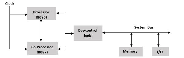
Fig: Block Diagram of Coprocessor configuration
Connection between processor and coprocessor
- The processor and coprocessor are connected via RQ-/GT-, TEST, QS0 and QS1 signals.
- TEST signal is connected to BUSY pin of coprocessor and the remaining 3 pins are connected to the same pins of the coprocessor.
- RQ-/GT- : This signal is used for the arbitration of bus.
- QS0 and QS1: These are used to track the status of the queue of the host processor.
- TEST: This signal is used to take care of the coprocessor?s activity i.e. the coprocessor is idle or busy.
Closely Coupled Configuration
Closely coupled configuration is exactly similar to the coprocessor configuration. Like coprocessor, it also shares the same memory, I/O system bus, and control logic and control generator with the host processor.
However, the host processor and the coprocessor fetch and execute their own instructions. The system bus is handled by the coprocessor and the host processor independently.
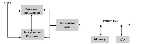
Fig: Block diagram of closely coupled configuration
How are the processor and independent processor connected?
- Memory space is used to provide the connection between independent processor and host processor.
- It does not use any instructions like WAIT, ESC etc. for communication.
- The host processor sends the commands to the ports for managing the memory and for waking up the independent processor.
- The independent processor accesses the memory and executes the task.
- When the task has been completed, it sends an acknowledgement to the host processor by using the status signal or an interrupt request.
Loosely Coupled Configuration
A loosely coupled multiprocessor configuration consists of the number of modules of the microprocessor based systems, which are connected through a common system bus. Each module of this configuration consists of their own clock generator, memory, I/O devices and is connected through a local bus.
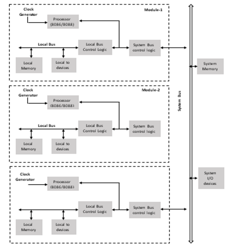
Fig: Block Diagram of loosely coupled configuration
8087 Numeric Data Processor
8087 numeric data processor is also known as Math Co-Processor, Floating point unit or Numeric processor extension.
It was first designed by Intel to pair with 8086/8088 resulting in easier and faster calculations.
Once the instructions are identified by the 8086/8088 processor, then it is sent to the 8087 co-processor for further execution.
The data types supported by Intel 8087 are:
- Binary integers
- Packed decimal numbers
- Real numbers
- Temporary real format
Features of 8087 numeric data processor
- It supports different data types like integer, float, and real types ranging from 2-10 bytes.
- It follows IEEE floating point standards.
- The processing speed is so high.
8087 Architecture
- 8087 architecture is divided into two group i.e.
- Control Unit (CU)
- Numeric Extension Unit (NEU)
- The Control Unit is responsible for all the communication between the processor and the memory such as it reads and writes memory operands, receives and decodes instructions, maintains parallel queue, etc.
- The Numeric Extension Unit (NEU) is responsible for all the numeric processor instructions like arithmetic, logical, transcendental, and data transfer instructions. It has 8 register stacks, which holds the operands for instructions and their results.
- CU and NEU works asynchronously with each other.
- Intel 8087 uses QS0 and QS1 pins to obtain and identify the instructions fetched by the host CPU.
- All the coprocessor instructions are identified by Escape (ESC) instructions code bits i.e. they start with 'F'. The coprocessor only executes the Escape instructions while other instructions are executed by the microprocessor.
- Once CPU recognizes ESC code, it triggers the execution of the numeric processor instruction in 8087.
- While executing, the ESC code identifies the coprocessor instruction that require memory operand or not. If the CPU does not require any memory operand, it will directly execute otherwise physical address of the operand is calculated using any one of the addressing modes allowed in 8086 and 1 dummy read cycle is initiated by the CPU.
- Then 8087 is ready with execution outputs, CU gets the control of bus from 8086 and executes a write cycle to write the outputs in the memory at the pre specialized address.
- Microcode control unit generates control signals required for execution of the instruction.
- Programmable shifter is used to shift the operands during the execution of instructions like FMUL and FDIV.
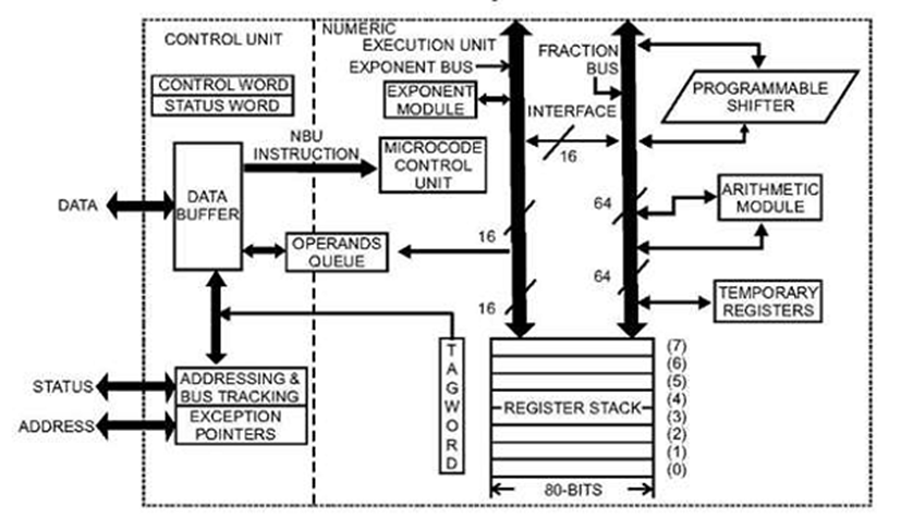
Fig: Architecture of 8087 Coprocessor
8087 Pin Description
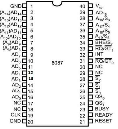
Fig: Pin diagram of Intel 8087
- AD0 - AD15: These are time multiplexed address/data lines, which carry addresses during T1 clock cycle and data during T2, T3, Tw and T4 clock cycles.
- A19/S6 - A16/S3: These are the time multiplexed address/status lines. These functions are similar to the pins of Intel 8086.
- BHE/S7: During the first clock cycle, it is used to enable data on to the higher byte of the 8086 data bus and after that during T2, T3, Tw and T4 clock cycles, it works as status line S7.
- QS1 - QS0: These are queue status input signal which is responsible for status of instruction queue.
Conditions of QS1 - QS0 are given below:

QS0 QS1 Status 0 0 No operation 0 1 1st byte of opcode from the queue 1 0 Empty the queue 1 1 Subsequent byte from the queue - INT: It is an interrupt signal used to indicate an unmasked exception has been received during the execution.
- BUSY (Output): When BUSY signal high then it indicates a busy state to the CPU.
- READY (input): This signal is used to reject the internal activities of the coprocessor and prepare it for further execution whenever required by the CPU.
- S0, S1, S2: These are the status signals which gives the status of the operation which is used by the Bus Controller 8087 to generate memory and I/O control signals.
S2 S1 S0 Status 0 X X Unused 1 0 0 Unused 1 0 1 Memory Read 1 1 0 Memory Write 1 1 1 Passive - RQ/GT1 and RQ/GT0: These are Request/Grant signals used by the 8087 processors to get the control of the bus from the host processor 8086/8088 for operand transfers.
- CLK (input): This input gives the basic timings for the processor operation.
- VCC: Power supply +5V.
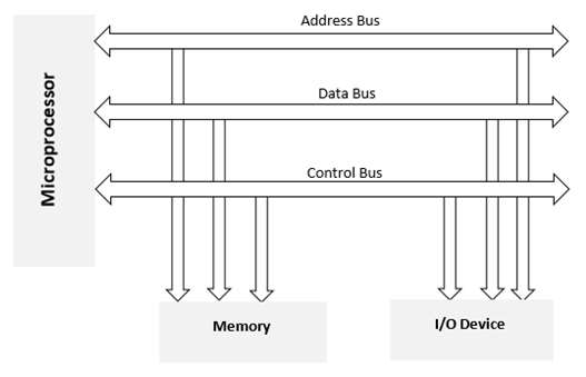
Memory and I/O Interfacing
Several memory chips and I/O devices are connected to a microprocessor.
The following figure shows a schematic diagram to interface memory chips and I/O devices to a microprocessor.
Memory Interfacing
When we are executing any instruction, the address of memory location or an I/O device is sent out by the microprocessor. The corresponding memory chip or I/O device is selected by a decoding circuit.
Memory requires some signals to read from and write to registers and microprocessor transmits some signals for reading or writing data.
The interfacing process includes matching the memory requirements with the microprocessor signals. Therefore, the interfacing circuit should be designed in such a way that it matches the memory signal requirements with the microprocessor's signals.
I/O interfacing
As we know, keyboard and displays are used as communication channel with outside world. Therefore, it is necessary that we interface keyboard and displays with the microprocessor. This is called I/O interfacing. For this type of interfacing, we use latches and buffers for interfacing the keyboards and displays with the microprocessor.
But the main drawback of this interfacing is that the microprocessor can perform only one function.
8279 Programmable Keyboard
The Intel 8279 is a programmable keyboard interfacing device. Data input and display are the integral part of microprocessor kits and microprocessor-based systems.
8279 has been designed for the purpose of 8-bit Intel microprocessors.
8279 has two sections namely keyboard section and display section.
The function of the keyboard section is to interface the keyboard which is used as input device for the microprocessor. It can also interface toggle or thumb switches.
The purpose of the display section is to drive alphanumeric displays or indicator lights. It is directly connected to the microprocessor bus.
The microprocessor is relieved from the burden of scanning the keyboard or refreshing the display.
Some important Features are:
- Simultaneous keyboard display operations
- Scanned sensor mode
- Scanned keyboard mode
- 8-character keyboard FIFO
- Strobed input entry mode
- 2-key lock out or N-key roll over with contact debounce
- Single 16-charcter display
- Dual 8 or 16 numerical display
- Interrupt output on key entry
- Programmable scan timing and mode programmable from CPU
8257 DMA Controller
The data transfer from fast I/O devices to the memory or from the memory to I/O devices through the accumulator is a time consuming process. For this situation, the Direct Memory Access (DMA) technique is preferred. In DMA data transfer scheme, data is directly transferred from an I/O device to RAM or from RAM to an I/O device.
Using a DMA controller, the device requests the CPU to hold its address, data and control bus, so the device is free to transfer data directly to/from the memory. The DMA data transfer is initiated only after receiving HLDA signal from the CPU.
How DMA operations are performed?
Following are the operations performed by a DMA:
- Initially, the device has to send DMA request (DRQ) to DMA controller for sending the data between the device and the memory.
- The DMA controller sends Hold request (HRQ) to the CPU and waits for the CPU for the HLDA.
- When CPU gets the HLDA signal then, it leaves the control over the bus and acknowledges the HOLD request through HLDA signal.
- Now the CPU is in the HOLD state and the DMA controller has to manage the operations over the buses between the CPU, memory and I/O devices.
Intel 8257
- The Intel 8257 is a programmable DMA controller.
- It is a 4-channel programmable Direct Memory Access (DMA) controller.
- It is a 40 pin I.C. package and requires +5V supply for its operation.
- It can perform three operations, namely read, write, and verify.
- Each channel incorporates two 16-bit registers, namely DMA address register and byte count register.
- Each channel can transfer data up to 64kb and can be programmed independently.
- It operates in 2 -modes: Master mode and Slave mode.
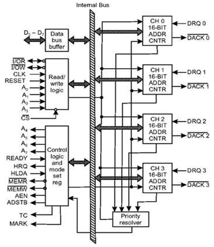
8257 Architecture
The following diagram is the architecture of Intel 8257:
8257 Pin Description
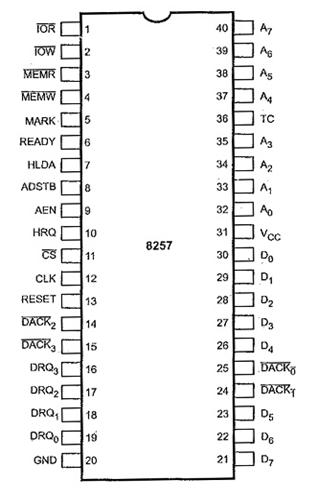
DRQ0 - DRQ3: These are DMA request lines. An I/O device sends the DMA request on one of these lines. On the line, a HIGH status generates a DMA request.
DACK0 - DACK3: These are DMA acknowledge lines. The Intel 8257 sends an acknowledge signal through one of these lines informing an I/O device that it has been selected for DMA data transfer. On the line, a LOW acknowledges the I/O device.
A0 - A7: These are address lines. A0 - A3 are bidirectional lines. These lines carry 4 LSBs of 16-bit memory address generated by the 8257 in the master mode. In the slave mode, these lines are all the input lines. The inputs select one from the registers to be read or programmed. A4 - A7 lines gives tristated outputs in the master mode which carry 4 through 7 of the 16-bit memory address generated by the Intel 8257.
D0 - D7: These are data lines. These are bidirectional three state lines. While programming the controller the CPU sends data for the DMA address register, the byte count register and the mode set register through these data lines.
AEN: Address latch enable.
ADSTB: A HIGH on this line latches the 8MSBs of the address, which are sent on D-bus, into Intel 8212 connected for this purpose.
CS: It is chip select.
(I/OR): I/O read. It is a bidirectional line. In output mode it is used to access data from the I/O device during the DMA write cycle.
(I/OW): I/O write. It is a bidirectional line. In output mode it allows the transfer of data to the I/O device during the DMA read cycle. Data is transferred from the memory.
MEMR: Memory read
MEMW: Memory write
TC: Byte count (Terminal count).
MARK: Modulo 128 Mark.
CLK: Clock
HRQ: Hold request
HLDA: Hold acknowledge
What is Microcontroller?
A microcomputer made on a single semiconductor chip is called single-chip microcomputer. Since, single chip microcomputers are generally used in control applications, they are also called microcontrollers.
Microcontroller contains all essential components of a microcomputer such as CPU, RAM, ROM/EPROM, I/O lines etc. Some single chip microcontrollers contain devices to perform specific functions such as DMA channels, A/D converter, serial port, pulse width modulation, etc.
8051 Architecture
In 1980, Intel introduced a powerful 8051 series of 8 -bit microcontrollers. They are the second generation of 8-bit microcontrollers. The 8051 microcontrollers are used for a variety of applications involving limited calculations and relatively some control strategies. They are used for industrial and commercial control applications, appliances control, instrumentation etc.
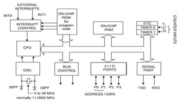
The 8051 contains Boolean processor, full duplex serial port and power saving circuitry in addition to essential components such as 8-bit CPU, RAM, ROM/EPROM/OTPROM, timer/counter and parallel I/O lines.
The following figure shows the block diagram or architecture of Intel 8051 microcontroller.
8051 Pins Description
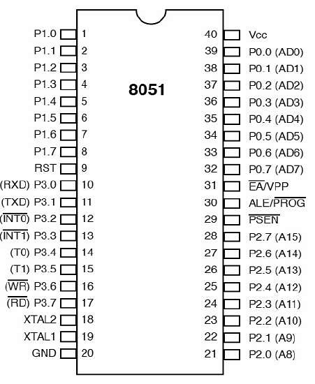
The pin diagram of 8051 microcontroller consists of 40 pins as given below:
Pin 1-8 (Port1): These are 8-bit bidirectional I/O port with internal pull-up resisters. It does not perform any task; it is just an I/O port
Pin 9 (RST): It is a Reset input pin which is used to reset the microcontroller to its initial position.
Pin 10 to 17 (Port 3): It is also an 8-bit bidirectional I/O port with internal pull-up resisters. Additionally, it performs some special functions:
PORT 3 Pin Function Description P3.0 RXD Serial Input P3.1 TXD Serial Output P3.2 INT0 External Interrupt 0 P3.3 INT1 External Interrupt 1 P3.4 T0 Timer 0 P3.5 T1 Timer 1 P3.6 WR External Memory Write P3.7 RD External Memory Read Pin 18 and 19: It is XTAL1 and XTAL1 pins respectively. These pins are used for connecting an external crystal to get the system clock.
Pin 20 (GND): It is a ground pin. It provides the power supply to the circuit.
Pin 21 to 28 (Port 2): These pins are bidirectional I/O port. Higher order address bus signals are multiplexed with this bidirectional port.
Pin 29 (PSEN): It is a Program Enable Pin. Using this PSEN pin external program memory can be read.
Pin 30 (ALE/PROG): This pin is the Address Latch Enable pin. Using this pin, external address can be separated from data.
Pin 31 (EA/VPP): Named as external Access Enable Pin (EA). It is used to enable or disable the external memory interfacing.
Pin 32 - 39 (Port 0): These are also a bidirectional I/O pins but without any internal pull-ups. Hence, it requires external pins in order to use port 0 pins as I/O port. Lower order data and address bus signals are multiplexed with this port.
Pin 40 (VCC): This pin is used to supply power to the circuit.
8051 I/O ports
8051 microcontroller have 4 I/O ports each of 8-bit, which can be configured as input or output. Hence, total 32 I/O pins allows the microcontroller to be connected with the peripheral devices.
Note: Pin can be configured as 0 for output and 1 for the input.
1) PORT 0
P0 can be used as a bidirectional I/O port or it can be used for address/data connected for accessing external memory. When control is 1 the port is used for address or data interfacing. When the control is 0 then the port can be used as a bidirectional I/O port.
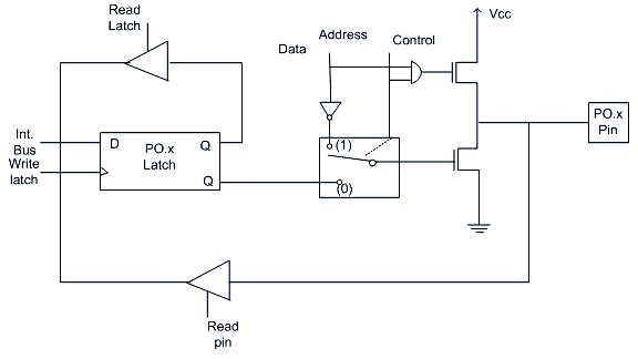
Fig: Structure of port 0 pin
PORT 0 as an Input Port
If the control is 0 then the port is used as an input port and 1 is written to the latch. In this type of situation both the output MOSFETs are off. Since the output pin has floats therefore, whatever data written on pin is directly read by read pin.
PORT 0 as an Output Port
If we want to write 1 on pin of P0, a '1' written to the latch which turns 'off' the lower FET while due to '0' control signal upper FET also turns off.
Suppose we want to write '0' on pin of port 0, when '0' is written to the latch, the pin is pulled down by the lower FET. Hence the output becomes zero.
2) PORT 1
PORT 1 is dedicated only for I/O interfacing. When used as an output port, not needed to connect additional pull-up resistor like port 0.
To use PORT 1 as an input port '1' has to be written to the latch. In this mode 1 is written to the pin by the external device then it read fine.
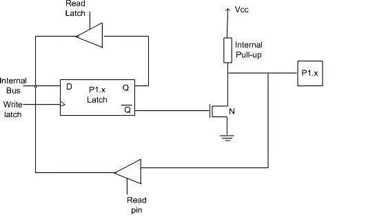
Fig: Structure of port 1 pin
3) PORT 2
PORT 2 is used for higher external address byte or a normal I/O port. Here, the I/O operation is similar to PORT 1. Latch of PORT 2 remains stable when Port 2 pin are used for external memory access.
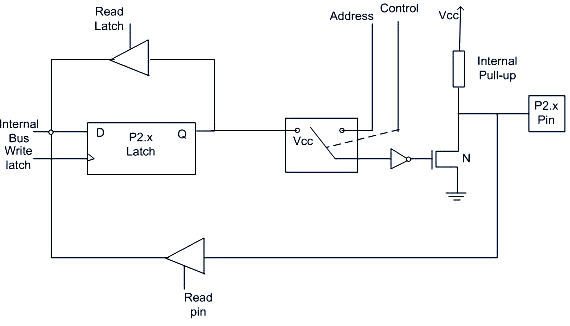
Fig: Structure of port 2 pin
4) PORT 3
Following are the alternate functions of PORT 3:
PORT 3 Pin Function Description P3.0 RXD Serial Input P3.1 TXD Serial Output P3.2 INT0 External Interrupt 0 P3.3 INT1 External Interrupt 1 P3.4 T0 Timer 0 P3.5 T1 Timer 1 P3.6 WR External Memory Write P3.7 RD External Memory Read It works as an I/O port same like port 2. Alternate functions of port 3 makes its architecture different than other ports.
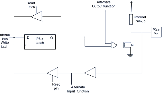
Fig: Structure of port 3 pin
8051 interrupts
Interrupt is a process of creating a temporary halt main program and pass the control to the external sources and execute their task and then passes the control to the main program where it held left off.
8051 has 5 interrupt signals, i.e.
- INT0,
- TFO,
- INT1,
- TF1,
- RI/TI.
The number of interrupt sources differs from version to version. It varies from 5 to 15.
The important interrupt sources are: one from the serial port, two from timers, two from external interrupts INT0 and INT1.
Each of the interrupts can individually be enabled/disabled by setting/clearing a bit in the special function register IE (interrupt enable). The IE register also contains a global disable bit, which disables all the interrupts.
Each interrupt can also be programmed to one of the priority level scheme by setting/clearing bits in the special function register IP (Interrupt Priority register).
A low priority interrupt can be interrupted by a high priority interrupt, but it cannot be interrupted by another low priority interrupt. A high priority interrupt can?t be interrupted by a low priority interrupt.
Difference between Microprocessor and Microcontroller
Microprocessors Microcontrollers It is used for big applications. It is used to execute a single task within an application. Microprocessor is the heart of computer system. It is the heart of the embedded system. It is just a processor. Memory and I/O components have to be having to be connected externally. Microcontroller contains external processor along with internal memory and I/O components. Since I/O and memory connected externally, the circuit becomes large. Since I/O and memory present internally, the circuit is small. Can't be used in compact systems and hence inefficient. Can be used in compact systems and microcontroller is an efficient technique. Cost of entire system increases. Cost of entire system is low. Power consumption is high. Power consumption is low. Most of the microprocessors do not have power saving modes. Most of the microcontrollers have power saving mode. Difficult to replace. Easy to replace. Mainly used in personal computers. Used mainly in washing machine, MP3 players. Peripheral Devices
To communicate with the outside world microcomputers use peripherals (I/O devices). Commonly used peripherals are: A/D converter, D/A converter, CRT, printers, Hard disks, floppy disks, magnetic tapes etc.
Peripherals are connected to the microcomputer through electronic circuits known as interfacing circuits.
Programmable Peripheral interface (PPI)
A programmable peripheral interface is a multiport device. The ports may be programmed in a variety of ways as required by the programmer. The device is very useful for interfacing peripheral devices. The term PIA, Peripheral Interface Adapter is also used by some manufacturer.
Intel 8255
The Intel 8255 is a programmable peripheral interface (PPI). It has two versions, namely the Intel 8255A and Intel 8255A-5. General descriptions for both are same. There are some differences in their electrical characteristics. Hereafter, they will be referred to as 8255. Its main functions are to interface peripheral devices to the microcomputer.
It has three 8-bit ports, namely Port A, Port B and Port C. The port C has been further divided into two 4-bit ports, port C upper and Port C lower. Thus a total of 4-ports are available, two 8-bit ports and two 4-bit ports. Each port can be programmed either as an input port or an output port.
Operating Modes of 8255
The Intel 8255 has the following three modes of operation which are selected by software:
Mode 0 - Simple Input/output: The 8255 has two 8-bit ports (Port A and Port B) and two 4-bit ports (Port Cupper and Port Clower). In Mode 0 operation, a port can be operated as a simple input or output port. Each of the 4 ports of 8255 can be programmed to be either an input or output port.
Mode 1-Strobed Input/output: Mode 1 is strobed input/output mode of operation. The Port A and Port B both are designed to operate in this mode of operation. When Port A and Port B are programmed in Mode 1, six pins of Port C are used for their control.
Mode 2 -Bidirectional Port: Mode 2 is strobed bidirectional mode of operation. In this mode Port A can be programmed to operate as a bidirectional port. The mode 2 operation is only for Port A. When Port A is programmed in Mode 2, the port B can be used either Mode 1 or Mode 0.
Architecture of Intel 8255
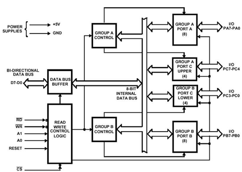
Intel 8255A pin description
It is a 40 pin I.C. package. It operates on a single 5 Vd.c. supply. Its important characteristics are as follows:
Ambient temperature 0 to 700C, Voltage on any pin: 0.5 V to 7 V. Power dissipation 1 Watt VIL = Input low voltage = Minimum 0.5 V, Maximum 0.8 V. VIH = Input high voltage = Minimum 2 V, Maximum Vcc. VOL = Output low voltage = 0.45 V VOH = Output High Voltage = 2.4 V IDR = Darlington drive connect = Minimum 1 mA, Maximum 4 mA of any 8 pins of the port.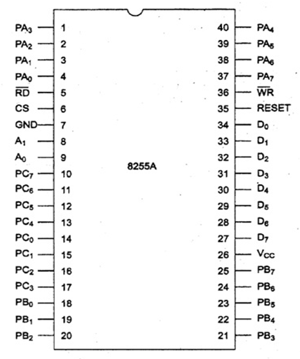
The pins of various ports are as follows:
PA0 - PA7 8 Pins of port A PB0 - PB7 8 pins of port B PC0 - PC3 4 pins of port Clower PC4 - PC7 4 pins of Port CupperThe important control signals are:
CS (Chip Select): It is a chip select signal. The LOW status of this signal enables communication between the CPU and 8255.
RD (READ): When RD goes LOW the 8255 sends out data or status information to the CPU on the data bus. In other words it allows the CPU to read data from the input port of 8255.
WR (Write): When WR goes LOW the CPU writes data or control word into 8255. The CPU writes data into the output port of 8255 and the control word into the control word register.
RESET: RESET is an active high signal. It clears the control register and sets all ports in the input mode.
A0 and A1: The selection of input port and control word register is done using A0 and A1 in conjunction with RD and WR. A0 and A1 are normally connected to the least significant bits of the address bus. If two 8255 units are used the addresses of ports are as follows:
For the First unit of 8255, i.e. 8255.1:
Port/Control word register Port/Control word register Address Port A 00 Port B 01 Port C 02 Control word register 03 For the 2nd unit of 8255, i.e. 8255.2:
Port/Control word register Port/Control word register Address Port A 08 Port B 09 Port C 0A Control word register 0B 8253 Programmable Interval Timer
A programmable counter/interval timer is used in real time application for timing and counting function such as BCD/binary counting, generation of accurate time delay, generation of square wave of desired frequency, rate generation, hardware/software triggered strobe signal, one shot signal of desired width etc.
Popular programmable interval timer chips are Intel 8253 and 8254. Both are pin to pin compatible and operate in the following six modes:
Mode 0: Interrupt on terminal count
Mode 1: Programmable one-shot
Mode 2: Rate generator
Mode 3: Square wave generator
Mode 4: Software triggered mode
Mode 5: Hardware triggered mode
The 8254 is compatible to 8086, 8088, 8085 and most other microprocessors. The 8253 is compatible to 8085 microprocessor. The 8254 is superset of the 8253.
Architecture of Intel 8253/54
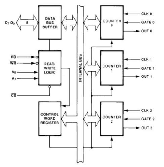
Intel 8253
The 8253 is 24-pin IC and operates at 5 Vd.c.. It contains three independent 16-bit counters. The programmer can program 8253 to operate in any one of the 6 operating modes. It operates under software control.
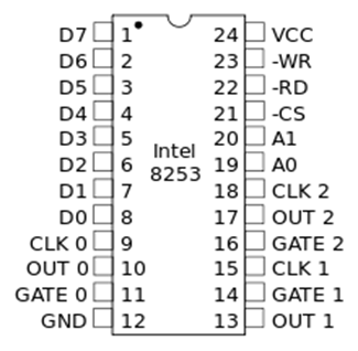
The description of its important pins is as follows:
RD (Read): When this pin is LOW the CPU reads data.
¯WR: (Write): When this is low, the CPU outputs data in the form of mode information or loading of counters.
A0, A1: These pins are connected to the address bus. These are used to select one of three counters. These are also used to address the control word registers for mode selection.
CS: Chip Select.
D0 - D7: Bidirectional data bus.
CLK0, CLK1 and CLK2 are clock for Counter 0, Counter 1 and Counter 2 respectively.
GATE0, GATE1 and GATE2 are gate terminals of Counter 0, Counter 1 and Counter 2 respectively.
OUT0, OUT1 and OUT2 are output terminals of Counter 0, Counter 1 and Counter 2 respectively.
The 8253 contains a data buffer, read/write logic and control word register as described below:
Data Bus Buffer: This buffer is within 8253. It is a 3-state, bidirectional, 8-bit buffer. It is used to interface 8253 to the system data bus through D0 - D7 lines.
Read/Write logic: The 8253 contains a read/write logic which accepts input from the system bus and then generates control signals for the operation of 8253. The following table shows the status of pins associated with read/write logic for various controls:
CS A1 A0 RD WR Result 0 0 0 0 1 Read Counter No. 0 0 0 1 0 1 Read Counter No. 1 0 1 0 0 1 Read Counter No. 2 0 0 0 1 0 Read Counter No. 0 0 0 1 1 0 Read Counter No. 1 0 1 0 1 0 Read Counter No. 2 0 1 1 1 0 Write Mode word 0 1 1 0 1 No-operation 3 state 0 X X 1 1 No-operation 3 state 0 X X X X Disable 3 -state Note: - X indicates undefined state. It means that it does not matter whether the state is 0 or 1.
Counter Word Register: When the pins A0, A1 are 11, the control word register is selected. The control word format is shown below:
D7 D6 D5 D4 D3 D2 D1 D0
SC1 SC0 RL1 RL0 M2 M1 M0 BCD The bits D7 and D6 of the control word are to select one of the 3 counters. D5 and D4 are for loading/reading the count. D3, D2 and D1 are for the selection of operating mode of the selected counter. These are six modes of operation for each counter of 8253. The six modes of operation are: MODE 0, MODE 1, MODE 2, MODE 3, MODE 4 and MODE 5. The bit D0 is for the selection of binary or BCD counting.
8253/54 Operational Modes
8253/54 can be operated in 6 different modes. These modes are:
MODE 0 : Interrupt on Terminal Count
- Mode 0 is used for the generation of accurate time delay under software control.
- One of the counters of 8253 is initialized and loaded with suitable count for the desired time delay.
- When counting is finished the counter interrupts the CPU. On interruption the microprocessor performs the required task which is to be performed after the desired time delay.
- For MODE 0 operation GATE is kept high. While counting is going on the counter output OUT remains LOW. When the terminal count is reached i.e. count reaches 0, the output becomes HIGH until the count is reloaded or new count is loaded.
- When the count is reloaded or OUT becomes LOW and the counter starts its counting operation again.
MODE 1 : Programmable One-Shot
- In MODE 1 the counter acts as a retriggerable and programmable one-shot.
- The LOW to HIGH transition of the signal applied to GATE acts as a trigger signal.
- In this mode of operation OUT becomes initially HIGH after the mode is set. After mode set operation the counter is loaded by a count value of N. The counter decrements count, and the output (OUT) goes LOW for N clock cycles for every LOW to HIGH transition of the GATE input.
MODE 2 : RATE Generator
- In MODE 2 the counter acts as a simple divide by N counter.
- When this mode is set the output of the counter becomes initially HIGH.
- After mode set operation the counter is loaded by a count of value N.
- For MODE 2 operation GATE is kept HIGH.
- In this mode the output remains HIGH for (N-1) clock pulses and then goes LOW for one clock pulse.
MODE 3 : Square Wave Generation
- In MODE 3 the counter acts as a square wave generator. After mode set operation the counter is loaded by a count of value N.
- For MODE 3 operation GATE is kept HIGH.
- For even values of N the output remains HIGH for N/2 clock pulses abd then goes LOW for next N/2 clock pulses.
MODE 4 : Software Triggered Strobe
- In MODE 4 operation the output of the counter becomes initially HIGH after the mode is set.
- GATE is kept HIGH for this mode of operation. The counter begins counting immediately after the count is loaded into the count register.
- When the counter reaches terminal count (i.e. counter content = 0) the output goes LOW for one clock period, then it returns to HIGH.
- The output signal may be used as strobe.
- This mode of operation is referred to as a software triggered strobe because the generation of the strobe signal is triggered by loading the count into the count register.
MODE 5 : Hardware Triggered Strobe
- In this mode of operation GATE input acts as a trigger.
- After the mode is set, the output becomes initially HIGH.
- A count value of N is loaded into the counter.
- Following a LOW to HIGH transition of the GATE input the counter starts decrementing the count.
- The counting begins at the first negative edge of the clock after the rising edge of the GATE input.
- On terminal count the output goes LOW for one clock period, and then it goes HIGH again.
- As the LOW to HIGH transition of the GATE input causes triggering, this mode is referred to as hardware triggered strobe.
Maximum mode and Minimum mode in 8086 Microprocessor
The 8086 microprocessor, advanced by Intel, was one of the most influential and extensively used microprocessors inside the early days of personal computing. It added a 16-bit architecture and served as the foundation for the x86 family of processors that keep dominating the marketplace these days. The 8086 microprocessor featured two working modes known as Maximum Mode and Minimum Mode, which provided exclusive levels of system configuration and control.
Maximum Mode:
The Maximum Mode of the 8086 microprocessor is supposed for use in structures where the processor is the significant element and has full control over the device bus. In this mode, the microprocessor acts because of the bus controller and interacts without delay with other gadgets together with memory, I/O ports, and co-processors. The Maximum Mode configuration calls for extra help chips, including the 8288 bus controller, to manipulate bus arbitration and generate control alerts.
Key features of the Maximum Mode consist of:
- Bus Control: The 8086 microprocessor takes control of the machine bus, permitting it to initiate and control all records transfers among diverse devices related to the gadget.
- Multiple Processors: The Maximum Mode supports the usage of a couple of processors, making it suitable for multiprocessor structures. Each processor is assigned specific obligations, and that they talk through shared memory.
- External Bus Controller: In Maximum Mode, an outside bus controller, such as the 8288, is required to address bus arbitration and generate bus manage indicators. This controller facilitates efficient statistics transfer and prevents conflicts amongst distinctive gadgets.
- Expanded Address and Data Lines: The Maximum Mode lets in the usage of all 20 cope with lines and sixteen records strains of the 8086 microprocessor, allowing admission to a larger memory space and extra great I/O abilities.
Minimum Mode:
The Minimum Mode of the 8086 microprocessor is designed for systems wherein the processor shares the gadget bus with different devices and does not act as the bus controller. This mode is commonly utilized in single-processor systems or while the device calls for fewer assets and a much less complex configuration.
Key features of the Minimum Mode encompass:
- Bus Controller: In Minimum Mode, the microprocessor relies on an outside bus controller, which includes the 8284 clock generator, to address bus control indicators and bus arbitration. The bus controller coordinates the activities of various devices linked to the machine bus.
- Single Processor: The Minimum Mode is generally used in unmarried-processor structures wherein the microprocessor is the number one processing unit and does not require the complexities related to multiprocessor structures.
- Limited Address and Data Lines: In Minimum Mode, most effective 16 address traces and 16 facts lines of the 8086 microprocessor are utilized, proscribing the reminiscence addressing skills and I/O options compared to the Maximum Mode.
- Reduced Complexity: The Minimum Mode configuration simplifies the machine design with the aid of offloading bus manager obligations to an external bus controller, decreasing the overall complexity and price of the gadget.
Choosing the correct mode relies upon the unique requirements of the system. The Maximum Mode is appropriate for big-scale systems with a couple of processors, massive reminiscence and I/O requirements, and the need for full control over the device bus. On the other hand, the Minimum Mode is favored for easier structures with a single processor and restrained useful resource requirements, where the microprocessor stocks the bus with different gadgets.
Difference between Maximum mode and Minimum mode in 8086 Microprocessor
Certainly! Here's a desk highlighting the key differences between Maximum Mode and Minimum Mode within the 8086 Microprocessor:
Feature Maximum Mode Minimum Mode Bus Control 8086 acts as bus controller and manages the gadget bus. 8086 does not act as a bus controller and relies on an external bus controller. Bus Controller Requires an external bus controller (e.G.8288) for bus arbitration and manipulate sign generation. Requires an external bus controller (e.G., 8284) for bus manage signal era and coordination. Address Lines Utilizes all 20 address traces for extended reminiscence addressing. Utilizes handiest sixteen cope with traces for limited reminiscence addressing. Data Lines Uses all 16 records strains for statistics switch. Uses the handiest 16 data traces for facts switch. Processor Supports a couple of processors for multiprocessor structures. Designed for unmarried-processor systems. System Control Full control over the device bus and gadgets linked to it. Share management of the device bus with other gadgets. System Complexity More complicated device design because of bus manipulation obligations and support chips. Simple gadget layout as bus manager is treated by means of an external bus controller. Memory and I/O Can get right of entry to a larger memory space and accommodate extra good sized I/O abilities. Limited reminiscence addressing and I/O options. System Cost Generally higher gadget value because of extra support chips. Lower machine fee due to reduced complexity and less aid chips. Typical Use Suitable for larger systems with more than one processor and sizable memory/I/O requirements. Preferred for simpler systems with an unmarried processor and restricted resource desires. These are the important differences between Maximum Mode and Minimum Mode in the 8086 Microprocessor. The preference among the 2 modes relies upon the particular necessities and complexity of the system being designed.
Memory mapped IO and IO mapped IO with reference to 8085 microprocessors
When it comes to interacting with outside gadgets, microprocessors utilize two number one strategies: reminiscence-mapped I/O and I/O-mapped I/O. These strategies play an essential position in managing input and output operations in a pc gadget. In the case of the 8085 microprocessor, information about the principles of memory-mapped I/O and I/O-mapped I/O is critical for effectively controlling peripheral gadgets.
Memory-Mapped I/O:
Memory-mapped I/O is a way of interfacing outside devices with a microprocessor by treating them as memory locations. In this technique, unique reminiscence addresses are reserved for I/O operations, and the microprocessor accesses those addresses to talk with the devices.
In the context of the 8085 microprocessor, a number of reminiscence addresses (normally referred to as I/O ports) is assigned for numerous input and output gadgets. These ports are accessed through the use of precise commands, together with IN and OUT instructions, which transfer statistics between the accumulator and the I/O ports.
For example, to examine data from a keyboard related to the 8085 microprocessor, a programmer can use the IN practice, specifying the I/O port deal with in which the keyboard facts are available. The records from the keyboard are then transferred to the accumulator, permitting further processing through the microprocessor.
I/O-Mapped I/O:
In contrast to memory-mapped I/O, I/O-mapped I/O assigns separate scope with areas for enter and output operations. The microprocessor uses specific instructions to have interaction with these addresses, which are special from the reminiscence addresses used inside the device.
In the case of the 8085 microprocessor, I/O-mapped I/O is not natively supported. However, with the help of sure deciphering strategies and additional circuitry, it's far feasible to enforce I/O-mapped I/O on the 8085.
The benefit of I/O-mapped I/O lies in the separation of memory and I/O addresses. This lets in for clearer differentiation between reminiscence access and I/O operations, enhancing system reliability and versatility.
Comparison and Selection:
Both reminiscence-mapped I/O and I/O-mapped I/O have their very own blessings and trade-offs. The preference between the 2 relies upon the precise necessities of the system and the to be had hardware.
Memory-mapped I/O simplifies the programming process by treating I/O gadgets as though they were reminiscence places. This lets programmers apply the same set of instructions for each reminiscence and I/O operations. However, it limits the quantity of to be had reminiscence addresses for other purposes, as some addresses are reserved for I/O.
On the opposite hand, I/O-mapped I/O presents a clearer separation between memory and I/O operations. This separation permits for large deals with spaces for reminiscence and I/O, decreasing the possibilities of conflicts among the two. However, it calls for extra deciphering circuitry and might involve greater complex programming techniques.
Difference between Memory mapped IO and IO mapped IO with reference to 8085 microprocessors
Certainly! Here's an increased table highlighting the differences among reminiscence-mapped I/O and I/O-mapped I/O within the context of 8085 microprocessors:
Aspect Memory-Mapped I/O I/O-Mapped I/O Addressing Devices treated as memory places Separate address area for I/O operations Address Range Shares memory addresses with gadget reminiscence Uses devoted addresses awesome from memory addresses Hardware Complexity Simpler, because it utilizes existing memory addressing mechanism Requires extra interpreting circuitry and complexity Instruction Set Same set of commands used for memory and I/O operations Different commands used for I/O operations Address Availability Limits the available reminiscence addresses for different functions Provides larger address spaces for reminiscence and I/O operations Clarity and Reliability May reason ambiguity and ability conflicts with memory Clearer separation between memory and I/O addresses Interrupt Handling Can share interrupt vectors with memory Requires separate interrupt vectors for I/O devices Priority Control Relies on software program-based priority control Easier hardware-primarily based precedence manipulate Flexibility Limited flexibility in allocating memory for I/O devices More bendy in allocating memory for I/O devices Port Expansibility Limited variety of I/O ports available Can accommodate a larger wide variety of I/O ports Memory Utilization Shares reminiscence area with I/O gadgets, decreasing to be had memory Dedicated deal with area permits maximum reminiscence usage Voltage drop and Potential difference

Voltage drop and potential difference are fundamental principles in electrical engineering that play an essential position in the knowledge and analysis of electrical circuits. These principles help engineers and technicians evaluate the conduct and efficiency of electrical systems, ensuring the right functioning of diverse devices and additives.
Potential Difference:
Potential distinction, also called voltage, refers back to the difference in electric powered potential among two factors in an electrical circuit. It is denoted by using the symbol "V" and is measured in volts (V). Electric potential is the amount of electric potential strength consistent with unit rate at a particular point in a circuit. When a rate actions from a point of better potential to some extent of decrease capability, it reports a capacity difference.
Potential difference can be the concept of using pressure that pushes electric powered charges through a circuit. It is chargeable for going with the flow of cutting-edge technology, that's the movement of electric expenses. In easy terms, capacity distinction creates an electrical strain that causes electrons to transport from one factor to another, thereby enabling the flow of power.
Voltage Drop:
Voltage drop refers back to the decrease in voltage that happens as cutting-edge flows via a conductor or an electrical element. It is measured in volts (V) and indicates the loss of electrical strength because of the resistance encountered by means of the present day. According to Ohm's law, voltage drop is immediately proportional to the modern passing via the conductor and the resistance of the conductor.
When contemporary flows via a conductor, it encounters resistance, which may be because of factors which include the conductor's material, duration, and move-sectional vicinity. This resistance converts electrical electricity into warmth, causing a discount inside the voltage. The voltage drop can be calculated using Ohm's regulation: V = I × R, wherein V represents the voltage drop, I represents the cutting-edge, and R represents the resistance.
Voltage drop is an essential consideration in electric circuit layout and analysis. Excessive voltage drop can cause a lower in the performance of electrical gadgets and might even motivate malfunctions or screw ups. It is specifically critical in programs where specific voltage stages are required, which includes digital circuits, power transmission, and distribution systems.
Mitigating Voltage Drop:
To reduce voltage drop and make certain the efficient operation of electrical systems, several measures may be taken:
- Use appropriate twine size: Selecting the proper gauge of twine with a good enough move-sectional area reduces resistance and subsequent voltage drop.
- Minimize conductor length: Shortening the length of conductors in a circuit reduces the overall resistance, for that reason lowering the voltage drop.
- Increase conductor size: Increasing the diameter of the conductor decreases its resistance, resulting in decreased voltage drop.
- Improve conductor cloth: Using conductors with better conductivity, such as copper, reduces resistance and voltage drop compared to materials like aluminum.
- Reduce load demand: Limiting the strength intake of electrical devices inside proper limits prevents excessive voltage drop.
Difference between Voltage drop and Potential difference
Certainly! Here's a desk highlighting the important thing differences between voltage drop and ability difference:
Voltage Drop Potential Difference Represents the decrease in voltage in a circuit Represents the distinction in electric ability Occurs due to resistance encountered via the modern-day Exists between points in an electrical circuit Measured in volts (V) Measured in volts (V) Calculated using Ohm's law (V = I × R) Calculated with the aid of subtracting the potentials of points Dependent on contemporary and resistance Independent of current and resistance Results inside the loss of electrical strength Provides the driving force for modern-day go with the flow Can be mitigated by means of the usage of larger twine sizes and shorter lengths of conductors Used to decide the drift of electrical fees Crucial attention for green circuit design and evaluation Essential for expertise electric behavior Can motive malfunctions or screw ups in electric devices Helps set up suitable voltage tiers Affects the operation of devices in a circuit Determines the float path of current Addressed by means of minimizing resistance and optimizing conductor length Addressed by way of selecting suitable twine gauge These points outline the distinctions among voltage drop and potential difference, emphasizing their personality traits and roles in electric circuits.
Comments
Post a Comment